High Speed PCB
Wenshu is a professional high speed PCB manufacturer in China. As 5G era is coming, high speed PCBs need more and more in different applications.
| Layer Count | 1-40layers |
| Board Thickness | 0.2-5.0mm |
| Copper Thickness | Min. 1/2 OZ, Max. 10 OZ |
| PTH Wall | 25um(1mil) |
| Maximum Board Size | 1100*500mm(43”*19”) |
| Min laser drilling size | 4mil |
Prototype to Full Turn-Key Assembly
Through-Hole Lead-Free Wave Soldering
Best Price, Genuine Components
Quality Accreditation ISO9001
-
Description
-
Specification
Wenshu is a professional high-speed PCB manufacturer based in China, with over 12 years of experience in the field. With the impending arrival of the 5G era, the demand for high-speed PCBs is escalating across diverse applications.
Benefit from our:
- Extensive Expertise: Our journey of over 12 years has equipped us with profound insights into high-speed PCB manufacturing.
- Flexibility: We proudly embrace projects of any size, offering no minimum order quantity for high-speed PCBs.
- Diverse Material Options: Taconic, Rogers, Arlon – our comprehensive stock ensures a wide array of materials to cater to your needs.
- Meticulous Inspection: Every PCB undergoes rigorous 100% E-test and AOI inspection to ensure unmatched quality.
- Rapid Turnaround: We provide a swift 24-hour quick turn service for your high-speed PCB prototypes, ensuring timely realization of your ideas.
In essence, high-speed PCB design revolves around scenarios where signal integrity starts to be influenced by various physical aspects of the circuit board, including layout, layer arrangement, interconnections, and packaging. Issues such as delay, crosstalk, reflection, and emission come into play.
Wenshu, your steadfast high-speed PCB supplier, boasts an engineering team with over two decades of collective design experience. Our global footprint is evident in our extensive client base of over 1000 customers worldwide.
At Wenshu, we offer various high-speed PCB design software options, including Altium Designer, Cadence Or CAD, Legacy PCAD, and Eagle (Altium Conversion). Let us know which software aligns with your project’s requirements.
The meticulous attention invested in these complexities sets high-speed PCB design apart. While simpler circuit boards may center around component placement and routing, high-speed PCB design focuses on precise trace placement, trace width, signal separation, and component selection.
Wenshu is committed to delivering excellence that transcends expectations. We’re here to transform your high-speed PCB design aspirations into reality, ensuring that every intricate detail is handled precisely.
| ltem | Capability |
|---|---|
| Layer Count | 1-40layers |
| Base Material | KB、Shengyi、ShengyiSF305、FR408、FR408HR、IS410、FR406、GETEK、370HR、IT180A、Rogers4350、Rogers4000、PTFE Laminates(Rogers series、Taconic series、Arlon series、Nelco series)、Rogers/Taconic/Arlon/Nelco laminate with FR-4 material (including partial Ro4350B hybrid laminating with FR-4) |
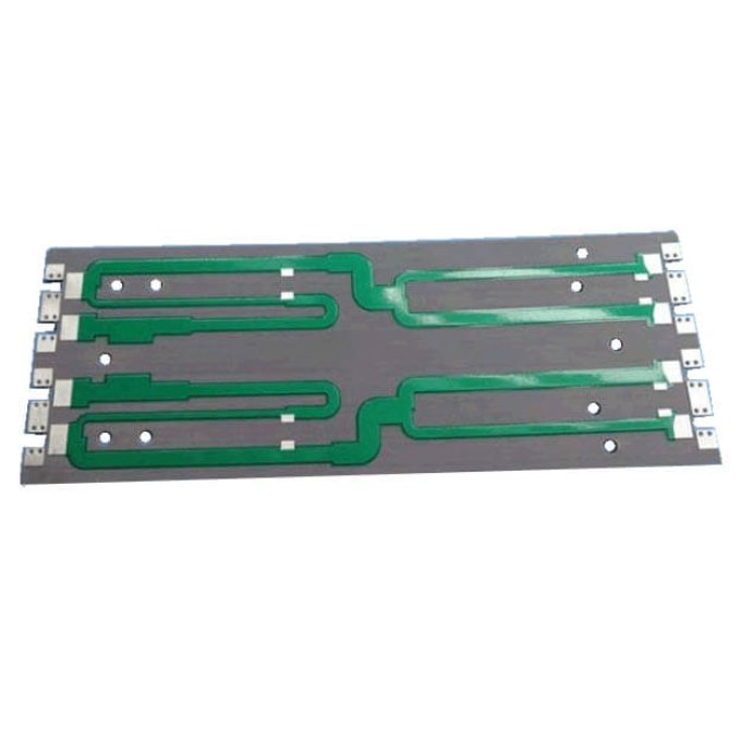
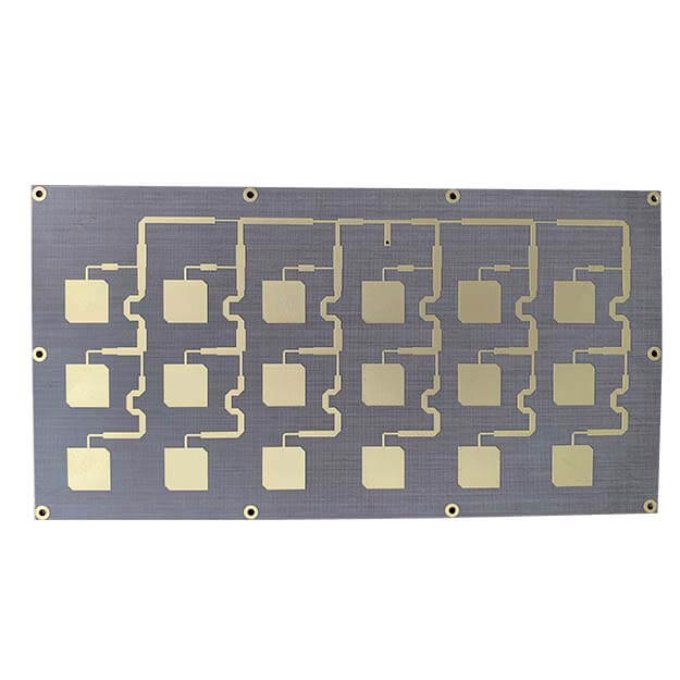
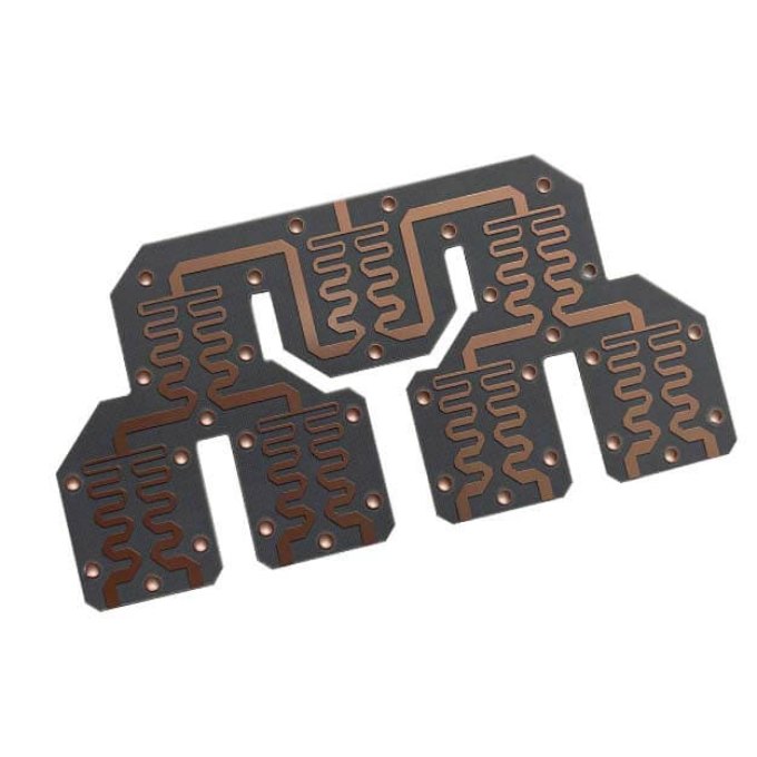
| Board Type | Backplane、HDI、High multi-layer blind&buried PCB、Embedded Capacitance、Embedded resistance board 、Heavy copper power PCB、Backdrill, PCB Gold Finger |
| Board Thickness | 0.2-5.0mm |
| Copper Thickness | Min. 1/2 OZ, Max. 10 OZ |
| PTH Wall | 25um(1mil) |
| Maximum Board Size | 1100*500mm(43”*19”) |
| Min laser drilling size | 4mil |
| Min.spacing/Tracing | 2.7mil/2.7mil |
| Solder Mask | Green, Black, Blue, Red, White, Yellow, Purple matte/glossy |
| Surface Treatment | Flash gold(electroplated gold)、ENIG、Hard gold、Flash gold、HASL Lead-free 、OSP、ENEPIG、Soft gold、Immersion silver、Immersion Tin、ENIG+OSP, ENIG+Gold finger, Flash gold(electroplated gold)+Gold finger(50u”), Immersion silver+Gold finger, Immersion Tin+Gold finger |
| Min. Annular Ring | 3mil |
| Aspect ratio | 10:1(HASL Lead-free 、HASL Lead、ENIG、Immersion Tin、Immersion silver、ENEPIG);8:1(OSP) |
| Impedance control | ±5ohm(<50ohm), ±10%(≥50ohm) |
| Other Techniques | Blind/Buried Via, Gold Fingers, Press Fit, Via in Pad, Electrical Test |