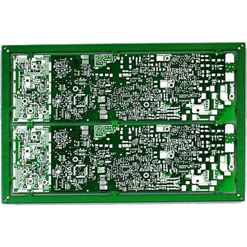
Medical Device PCB Board
Extra care must be taken to ensure reliability when producing medical PCBs. This is because human life depends on the equipment that houses them. PCBs also have to meet very strict requirements when it comes to cleanliness. This is especially true for those used in implants. First, they must be hygienic. They also have to be more compact than usual. Therefore, HDI (High Density Interconnect) PCBs are used in most medical devices.
| Plate | Shengyi S1000H |
| Plate thickness | 1.6mm |
| Size | 216.3*92.6mm |
| Minimum aperture | 0.1mm |
| Line width/moment | 0.1/0.1mm |
| Surface treatment | Immersion silver |
Prototype to Full Turn-Key Assembly
Through-Hole Lead-Free Wave Soldering
Best Price, Genuine Components
Quality Accreditation ISO9001
-
Description
-
Specification
Introducing the Medical Device PCB Board: A Game-Changer in Healthcare
The Medical Device PCB Board, or simply PCB, is a super important part of technology making a big impact. It’s used in things like smartphones, computers, and even devices for artificial intelligence. And guess what? It’s also changing the way medical stuff works!
These special PCBs are doing some amazing things in the medical world. They’re helping doctors and patients connect better, which is cool. These PCBs are like the magic behind new medical gadgets that are easy to use and helpful.
Medical PCBs are like the secret ingredient in making devices that can accurately figure out what’s wrong with you and keep an eye on your health. They’re making medical technology better and solving important problems in healthcare.
The part of the world where medical stuff meets technology is growing fast, and these PCBs are a big reason for it. People think that by 2022, the market for medical electronics will be worth billions! As technology improves, these PCBs become even more crucial for medical stuff to work correctly.
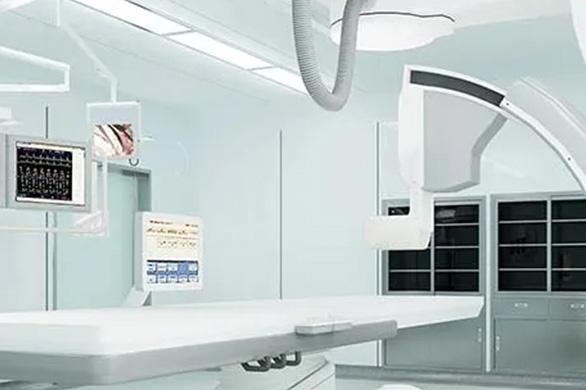
Picture this: heart monitors, X-ray machines, and other important medical devices. They all rely on PCBs to work perfectly. And it’s not just big machines; even blood pressure monitors use these special boards.
The people who make medical PCBs have to be extra careful because they’re dealing with things that affect human lives. When it comes to stuff inside our bodies, like implants, they need to be super clean and small. That’s why they use special technology called HDI PCBs.
There are some fancy techniques used to put these PCBs together. One is called via-in-pad technology, where they put tiny connections inside copper pads. Another cool thing is Surface Mount Technology, which helps make things smaller and work better.
| ltem | Capability |
|---|---|
| Layer Count | 1-40layers |
| Base Material | KB、Shengyi、ShengyiSF305、FR408、FR408HR、IS410、FR406、GETEK、370HR、IT180A、Rogers4350、Rogers4000、PTFE Laminates(Rogers series、Taconic series、Arlon series、Nelco series)、Rogers/Taconic/Arlon/Nelco laminate with FR-4 material (including partial Ro4350B hybrid laminating with FR-4) |
| Board Type | Backplane、HDI、High multi-layer blind&buried PCB、Embedded Capacitance、Embedded resistance board 、Heavy copper power PCB、Backdrill, PCB Gold Finger |
| Board Thickness | 0.2-5.0mm |
| Copper Thickness | Min. 1/2 OZ, Max. 10 OZ |
| PTH Wall | 25um(1mil) |
| Maximum Board Size | 1100*500mm(43”*19”) |
| Min laser drilling size | 4mil |
| Min.spacing/Tracing | 2.7mil/2.7mil |
| Solder Mask | Green, Black, Blue, Red, White, Yellow, Purple matte/glossy |
| Surface Treatment | Flash gold(electroplated gold)、ENIG、Hard gold、Flash gold、HASL Lead-free 、OSP、ENEPIG、Soft gold、Immersion silver、Immersion Tin、ENIG+OSP, ENIG+Gold finger, Flash gold(electroplated gold)+Gold finger(50u”), Immersion silver+Gold finger, Immersion Tin+Gold finger |
| Min. Annular Ring | 3mil |
| Aspect ratio | 10:1(HASL Lead-free 、HASL Lead、ENIG、Immersion Tin、Immersion silver、ENEPIG);8:1(OSP) |
| Impedance control | ±5ohm(<50ohm), ±10%(≥50ohm) |
| Other Techniques | Blind/Buried Via, Gold Fingers, Press Fit, Via in Pad, Electrical Test |