-
Capability
-
HDI PCB Capabilities
| ltem | Capability |
|---|---|
| Material | FR-4 Standard Tg 140°C, FR4-High Tg 170°C |
| Min. Track/Spacing | For External layers: 4oz Cu 10mil/13mil, 5oz Cu 12mil/15mil, 6oz Cu 15mil/15mil For Internal layers: 4oz Cu 8mil/8mil, 5oz Cu 10mil/10mil, 6oz Cu 12mil/12mil |
| Min. Hole Size | 0.15 ~ 0.3mm |
| Max Outer Layer Copper Weight (Finished) | 12oz |
| Max Inner Layer Copper Weight | 12oz |
| Board Thickness | 0.6-6mm |
| Surface Finishing | HASL lead-free, Immersion gold, OSP, Hard Gold, Immersion Silver, Enepig |
| Solder Mask | Green, Red, Yellow, Blue, White, Black, Purple, Matte Black, Matte green |
| Silkscreen | White, Black |
| Via Process | Tenting Vias, Plugged Vias, Vias not covered |
| Testing | Fly Probe Testing (Free) and A.O.I. testing |
| Build time | 5-15 days |
| Lead time | 2-3 days |
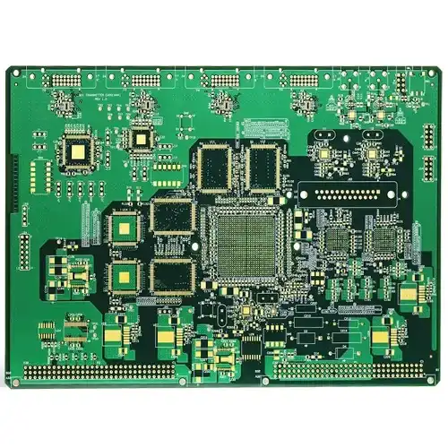
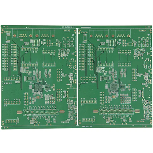
Rapidly gaining momentum, HDI PCB fabrication stands as the ultimate solution to craft PCBs that are smaller, more efficient, and exceptionally durable. High-Density Interconnect (HDI) represents a high-performance design with intricate component placement and sophisticated routing. This involves techniques like micro vias, blind and buried vias, and micro via methods, in conjunction with built-up printed circuit board (PCB) laminations.
With a specialization in HDI PCBs, Wenshu has extensive experience producing these advanced PCBs for diverse industries, including medical, automotive, and electronics. Our proficiency enables us to handle all HDI PCB projects, ensuring unmatched precision and superior quality while adhering to your budget constraints.


