-
Capability
-
PCB Prototype Capabilities
| ltem | Capability |
|---|---|
| Material | FR-4 Standard Tg 140°C, FR4-High Tg 170°C |
| Min. Track/Spacing | For External layers: 4oz Cu 10mil/13mil, 5oz Cu 12mil/15mil, 6oz Cu 15mil/15mil For Internal layers: 4oz Cu 8mil/8mil, 5oz Cu 10mil/10mil, 6oz Cu 12mil/12mil |
| Min. Hole Size | 0.15 ~ 0.3mm |
| Max Outer Layer Copper Weight (Finished) | 12oz |
| Max Inner Layer Copper Weight | 12oz |
| Board Thickness | 0.6-6mm |
| Surface Finishing | HASL lead-free, Immersion gold, OSP, Hard Gold, Immersion Silver, Enepig |
| Solder Mask | Green, Red, Yellow, Blue, White, Black, Purple, Matte Black, Matte green |
| Silkscreen | White, Black |
| Via Process | Tenting Vias, Plugged Vias, Vias not covered |
| Testing | Fly Probe Testing (Free) and A.O.I. testing |
| Build time | 5-15 days |
| Lead time | 2-3 days |
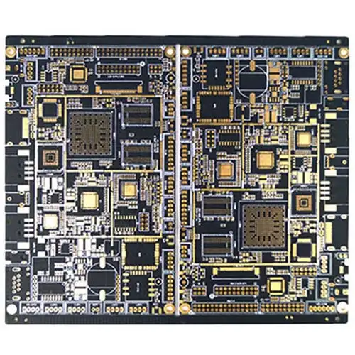
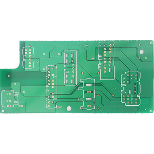
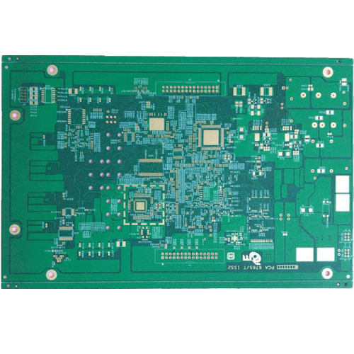
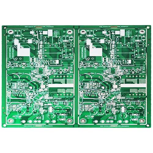
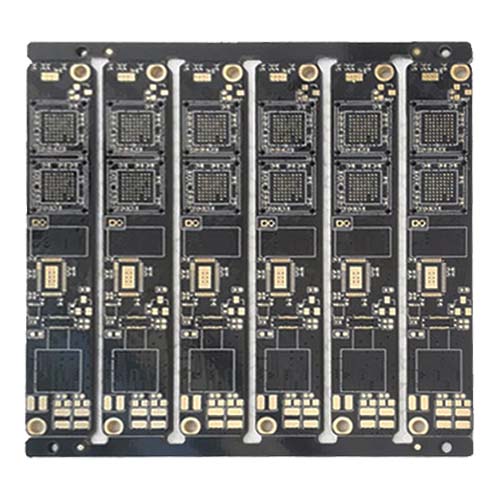
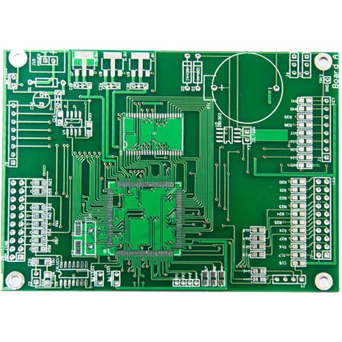
Presenting our cutting-edge solution: the PCB Prototype, designed to revolutionize rapid circuit prototyping and development. Seamlessly integrating with leading design software, it simplifies the transfer of your circuit schematics and layouts.
Our team of dedicated experts is poised to guide you through the entire PCB prototyping process. Whether you need technical insights, design assistance, or help with your order, our knowledgeable support staff is committed to your success.
Unleash the full potential of our PCB Prototype and fast-track your product development journey. Covering everything from concept to reality, we offer high-quality, swift, and customizable PCB prototypes tailored to your exact specifications.


