-
Capability
-
Standard PCB Capabilities
| ltem | Capability |
|---|---|
| Layer Count | 1-40layers |
| Base Material | KB、Shengyi、ShengyiSF305、FR408、FR408HR、IS410、FR406、GETEK、370HR、IT180A、Rogers4350、Rogers4000、PTFE Laminates(Rogers series、Taconic series、Arlon series、Nelco series)、Rogers/Taconic/Arlon/Nelco laminate with FR-4 material (including partial Ro4350B hybrid laminating with FR-4) |
| Board Type | Backplane、HDI、High multi-layer blind&buried PCB、Embedded Capacitance、Embedded resistance board 、Heavy copper power PCB、Backdrill, PCB Gold Finger |
| Board Thickness | 0.2-5.0mm |
| Copper Thickness | Min. 1/2 OZ, Max. 10 OZ |
| PTH Wall | 25um(1mil) |
| Maximum Board Size | 1100*500mm(43”*19”) |
| Min laser drilling size | 4mil |
| Min. Spacing/Tracing | 2.7mil/2.7mil |
| Solder Mask | Green, Black, Blue, Red, White, Yellow, Purple matte/glossy |
| Surface Treatment | Flash gold(electroplated gold)、ENIG、Hard gold、Flash gold、HASL Lead-free 、OSP、ENEPIG、Soft gold、Immersion silver、Immersion Tin、ENIG+OSP, ENIG+Gold finger, Flash gold(electroplated gold)+Gold finger(50u”), Immersion silver+Gold finger, Immersion Tin+Gold finger |
| Min. Annular Ring | 3mil |
| Aspect ratio | 10:1(HASL Lead-free 、HASL Lead、ENIG、Immersion Tin、Immersion silver、ENEPIG);8:1(OSP) |
| Impedance control | ±5ohm(<50ohm), ±10%(≥50ohm) |
| Other Techniques | Blind/Buried Via, Gold Fingers, Press Fit, Via in Pad, Electrical Test |
Complex Electronic Circuits Demand Standard PCBs
The intricacies of electronic appliances necessitate intricate electronic circuits. Designers must meticulously arrange minuscule electronic components onto an electronic board. This board, made of plastic, features copper tracks on one side and perforations for component placement.
Defining Standard PCBs
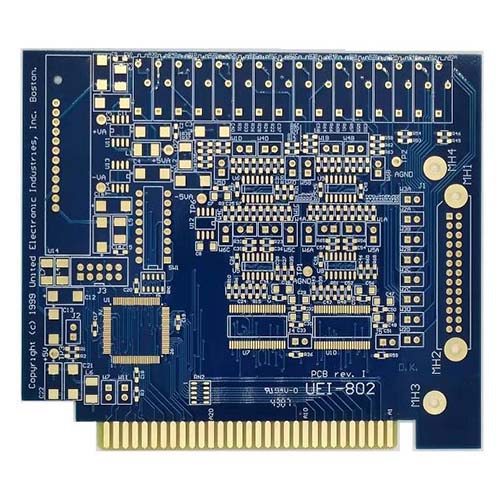
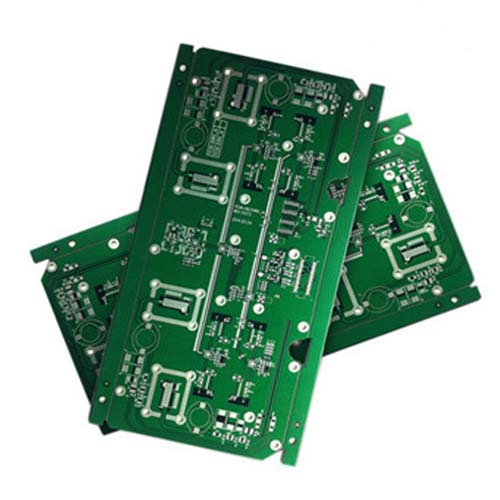
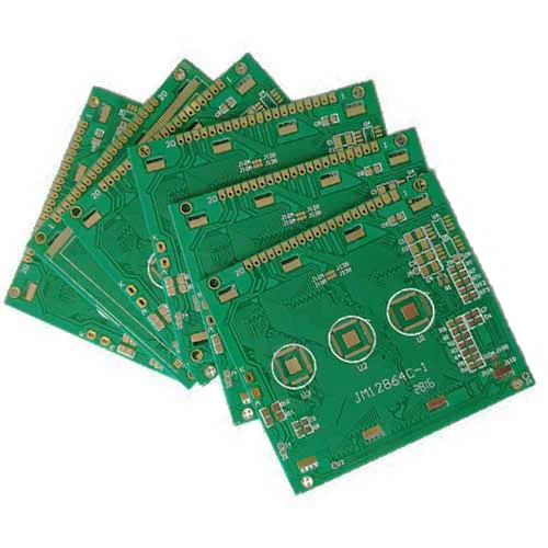
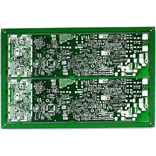
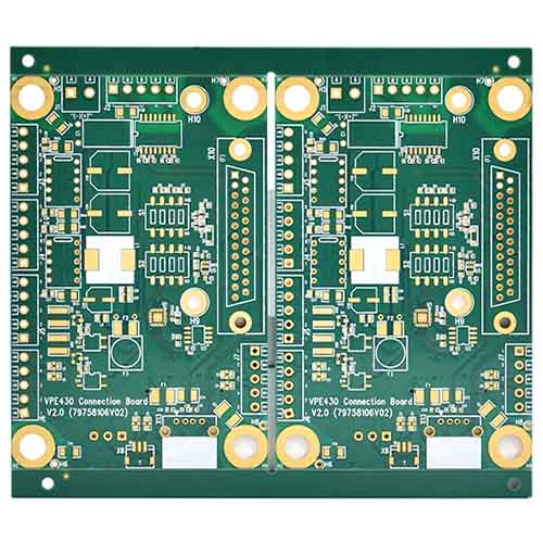
When a circuit pattern is etched onto a plastic board, it earns the title of a standard PCB. This unassuming component lies at the heart of diverse electronic devices, spanning from household gadgets to toys. Its significance pervades numerous applications, and its design permits mass production.
Advanced Skills for Assembly
Assembling electronic components requires advanced skills to meet the burgeoning demands of the market. This expertise is integral to accommodating a vast and ever-expanding market.
Unraveling Standard PCB Thickness
The historical standard PCB thickness stands at 1.60mm or approximately 0.062 inches, reflecting the size of early bakelite sheets used in fabrication. Although contemporary boards vary in size, this standard remains prevalent. A range of common thicknesses now exists, including 0.031 inches (0.80mm), 0.062 inches (1.60mm), and 0.093 inches (2.40mm). Your choice of fabrication and assembly services can yield boards of differing thicknesses.
Adapting to Applications
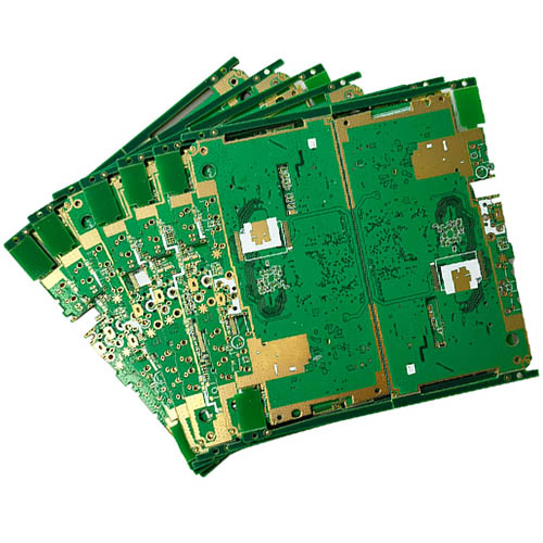
The diversity of applications calls for various types of PCB circuits. Single-sided and double-sided boards are commonly sought after, while multilayer and aluminum-supported ones shouldn’t be overlooked. PCBs vary in accordance with working frequencies, current power, and application-specific needs.
Customized Approach to Design and Construction
Creating these circuits demands tailored approaches. Monolayer (single-sided) PCBs are simplest and economical, while double-sided boards present more versatility. Multilayer circuits, comprising conductive layers, are notably intricate to craft.
Guided by Technology
Design and construction phases are monitored via dedicated equipment and computers. Adherence to customer specifications is imperative, while stringent assessments secure conformity certificates.


