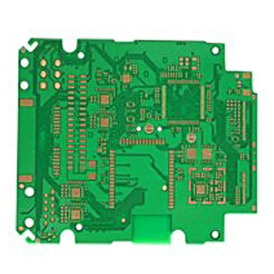
10-Layer FR4 PCB
We manufacture a 10-layer FR4 rigid PCB with a board thickness of 1.6 mm and a copper thickness of 1 OZ. These PCBs have a minimum hole size of 5 mils and a minimum line width of 4 mils. These PCBs do not have silkscreen but have green solder masks. Other solder mask color options include black, white, blue and red. The aspect ratio of these printed circuit boards is 10:1. Other material options for these printed circuit boards include Nelco, Getek, PTFE, Polyimide, CEM3, Halogen Free, Rogers and Teflon.
| Layers | 10 layers |
| Material | FR-4 |
| Plate thickness | 2.0mm |
| Minimum aperture | 0.1mm |
| Outer line width/line spacing | 4/4mil |
| Surface treatment | Immersion Gold |
Prototype to Full Turn-Key Assembly
Through-Hole Lead-Free Wave Soldering
Best Price, Genuine Components
Quality Accreditation ISO9001
-
Description
-
Specification
Introducing the 10-Layer FR4 PCB: Pinnacle of Multilayer Performance
Step into the future of printed circuit boards with our remarkable 10-layer FR4 PCB – a testament to innovation, precision, and advanced technology. This multilayer marvel is designed to elevate your electronic projects to new heights and opens doors to unparalleled possibilities across industries.
Key Features:
- Multilayer Complexity: Experience the power of 10 layers intricately interwoven into a single PCB. This exceptional layer count allows for intricate routing, intricate power distribution, and effective noise isolation, making it an ideal choice for complex and high-performance applications.
- Enhanced Signal Integrity: Our 10-layer FR4 PCB is engineered to deliver pristine signal integrity. The carefully designed stack-up ensures minimized crosstalk, reduced electromagnetic interference, and unmatched clarity in data transmission.
- Precision Thermal Management: Heat dissipation reaches new levels with the 10-layer FR4 PCB. The multiple planes provide optimal thermal paths, effectively managing heat generation and ensuring reliable operation even under demanding conditions.
- High-Density Components: Embrace the power of high-density design. The 10-layer configuration offers ample space for densely packed components without compromising performance, enabling you to create sleek and powerful electronic systems.
- Application Versatility: The 10-Layer PCB shines across various applications, from telecommunications infrastructure to advanced medical equipment. Its adaptability makes it a cornerstone of innovation in aerospace, automotive, and beyond industries.
- Unwavering Reliability: Crafted from the finest FR4 materials, this PCB stands as a symbol of reliability. Its robust construction ensures stability in challenging environments, guaranteeing longevity and consistent performance.
- Design Flexibility: With ten layers, your design possibilities are limitless. Customize your layout to optimize power distribution, impedance control, and routing efficiency, giving you the creative freedom to engineer exceptional solutions.
- Seamless Integration: The standardized form factor and compatibility with industry-standard components and connectors ensure seamless integration into your existing projects, streamlining the development process.
| Feature | Capability |
|---|---|
| Material | FR-4 Standard Tg 140°C, FR4-High Tg 170°C |
| Min. Track/Spacing | For External layers: 4oz Cu 10mil/13mil, 5oz Cu 12mil/15mil, 6oz Cu 15mil/15mil For Internal layers: 4oz Cu 8mil/8mil, 5oz Cu 10mil/10mil, 6oz Cu 12mil/12mil |
| Min. Hole Size | 0.15 ~ 0.3mm |
| Max Outer Layer Copper Weight (Finished) | 12oz |
| Max Inner Layer Copper Weight | 12oz |
| Board Thickness | 0.6-6mm |
| Surface Finishing | HASL lead-free, Immersion gold, OSP, Hard Gold, Immersion Silver, Enepig |
| Solder Mask | Green, Red, Yellow, Blue, White, Black, Purple, Matte Black, Matte green |
| Silkscreen | White, Black |
| Via Process | Tenting Vias, Plugged Vias, Vias not covered |
| Testing | Fly Probe Testing (Free) and A.O.I. testing |
| Build time | 5-15 days |
| Lead time | 2-3 days |


