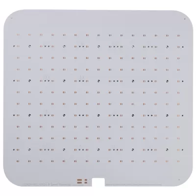
Plant Lamp PCB
The Plant PCB features a high-quality substrate material that ensures durability and thermal management. It is designed to accommodate various components such as LEDs, drivers, and control circuitry. Moreover, it enables precise control over light intensity, spectrum, and timing.
| Model | growth light pcb05 |
| Base material | aluminum |
| Board thick | 1.0/1.2/1.6mm |
| Copper thick | 0.5-3oz |
| Component type | patch ThT DIP |
| Surface treatment | HASL Leadless |
Prototype to Full Turn-Key Assembly
Through-Hole Lead-Free Wave Soldering
Best Price, Genuine Components
Quality Accreditation ISO9001
-
Description
-
Specification
Introducing the Plant Lamp PCB – an intricately crafted circuit board meticulously tailored to cater to the precise needs of plant growth and cultivation. Engineered for indoor plant environments, this PCB is dedicated to furnishing optimal lighting conditions. Furthermore, it serves as a dependable and streamlined answer for horticultural lighting systems.
Distinguishing itself with a top-tier substrate material, the Plant PCB ensures not only durability but also adept thermal management. Its design accommodates an array of components, including LEDs, drivers, and control circuitry. This holistic design approach grants meticulous command over aspects such as light intensity, spectrum distribution, and timing.
Highlights of the Plant Lamp PCB:
- Personalized Illumination Parameters: The PCB stands out by granting the power to tailor lighting parameters in accordance with specific plant prerequisites. This encompasses the fine-tuning of light intensity, spectral output, and photoperiod. The goal is to emulate natural sunlight, thereby optimizing plant maturation across various growth stages.
- Ingenious Power Governance: Skillfully integrating energy-efficient techniques, the PCB expertly manages power distribution. By enabling pinpoint control over power allocation, it diminishes energy wastage – ultimately translating to reduced electricity expenses and a notable boost in environmental sustainability.
- Ingenious Thermal Regulation: The Plant PCB has been engineered with keen thermal management features, primed to swiftly dissipate heat. This functionality is pivotal in sustaining optimal operating temperatures for the integrated LEDs and other components. Such precise thermal control contributes to elongated lifespans while circumventing the perils of overheating.
- Unwavering Circuit Safeguards: Infused with circuit protection mechanisms encompassing overcurrent and overvoltage safeguards, the PCB functions as a barrier against electrical surges and anomalies. This fortified design fosters a landscape of durability and safety for the entire plant lamp ecosystem.
- Seamless Integration and Expandability: Designed to seamlessly integrate within expansive lighting frameworks or stand-alone plant luminaires, the Plant Lamp PCB accommodates various scales and growth requirements. This innate adaptability ensures a harmonious fit regardless of plant dimensions or cultivating area.
By investing in the Plant Lamp PCB, one opens the gateway to crafting efficient and bespoke lighting solutions for indoor plants. This progressive PCB technology equally empowers enthusiasts engaged in horticulture pursuits.
| Feature | Capability |
|---|---|
| Material | FR-4 Standard Tg 140°C, FR4-High Tg 170°C |
| Min. Track/Spacing | For External layers: 4oz Cu 10mil/13mil, 5oz Cu 12mil/15mil, 6oz Cu 15mil/15mil For Internal layers: 4oz Cu 8mil/8mil, 5oz Cu 10mil/10mil, 6oz Cu 12mil/12mil |
| Min. Hole Size | 0.15 ~ 0.3mm |
| Max Outer Layer Copper Weight (Finished) | 12oz |
| Max Inner Layer Copper Weight | 12oz |
| Board Thickness | 0.6-6mm |
| Surface Finishing | HASL lead-free, Immersion gold, OSP, Hard Gold, Immersion Silver, Enepig |
| Solder Mask | Green, Red, Yellow, Blue, White, Black, Purple, Matte Black, Matte green |
| Silkscreen | White, Black |
| Via Process | Tenting Vias, Plugged Vias, Vias not covered |
| Testing | Fly Probe Testing (Free) and A.O.I. testing |
| Build time | 5-15 days |
| Lead time | 2-3 days |


